


Design of Uninterruptible
Power Supply/UPS
Problem Statement:
Design a 1kVA UPS powered by
a single phase 220V/50Hz AC. You may consider one of the following design
options:
a. A rectifier as battery charger+ DC-DC Boost converter +
Sinusoidal PWM Inverter
b. A rectifier as battery charger + Full bridge DC-DC converter
using pulse power transformer+ Sinusoidal PWM Inverter
c. A
rectifier as battery charger + Sinusoidal PWM Inverter + Step up transformer
Charging current of battery
must not exceed 15A and you must take care of input power factor.
What is an Uninterruptible Power
Supply?
An uninterruptible
power supply, also uninterruptible power source, UPS or battery/flywheel backup is an
electrical apparatus that provides power to the system which it is connected to
i.e household assembly of electricity run devices, offices, computer run etc
when the power from the main grid gets disrupted or cut off and it can also
provide emergency power to a load when the input power source, typically mains power, fails.
UPS is a device that provides battery backup when the electrical
power fails or drops to an unacceptable voltage level. Small UPS systems
provide power for a few minutes; enough to power down the computer in an
orderly manner, while larger systems have enough battery for several hours. In
mission critical data centers, UPS systems are used for just a few minutes until
electrical generators take over.
UPS systems can be set up to alert file servers to shut down
in an orderly manner when an outage has occurred, and the batteries are running
out.
What is
the working Principle of Uninterrupted Power Supply?
From basic principles in terms of application, UPS is a
device that contains stored energy in order to inverter as the main component,
regulated stable frequency and output power protection equipment mainly by the
rectifier, batteries, power inverters and static switch of several components.
11) Rectifier:
Rectifier is a rectifier device, simply means
that the exchange of (AC) into direct current (DC) devices. It has two main
functions: First, the alternating current (AC) into direct current (DC),
through the supply of filtered load, or the supply inverter; second, to provide
battery charging voltage. Therefore, it is also play a role in charger.
22)
Battery:
UPS battery is used as a storage energy device,
which consists of several cells in series, with a capacity to maintain its size
determines the discharge (supply) time. Its main function is: When the
electricity is normal, the energy converted into chemical energy stored in the
battery internal; when the electricity fails, the chemical energy into
electrical energy provided to the inverter or the load.
33)
Inverter:
The inverter
is a DC (DC) into alternating current (AC) device. It consists of inverter bridge control logic and filter circuit.
Which design have to chosen?
We have designed the battery charger using step-down
transformer, rectifier and buck converter as battery charger. For converting
battery power into AC we have used H-bridge circuit as square wave generator
for pulse transformer whose output is fed to the Bridge rectifier which
converts this square wave into an almost constant DC potential which is then
fed into the inverter which will convert this DC potential into a Sinusoidal AC
waveform.
What is the logic behind choosing this design?

Design of Step Down Transformer
For our design we are taking a 220v to 100v step down transformer
Here we have not taken the small value of secondary voltage
to minimize the effect of poor power factor and harmonic distortion. The reason behind not taking a very high
secondary voltage is to avoid high ratings of our transformer.

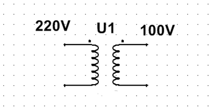
Fig.
1 Step-down Transformer
Buck Converter Design
We assume that battery takes 12A as maximum current for charging.

Fig.
2 Buck converter feeding the Battery
Now if we have 16V at the output of
Buck converter along with 0.2V of ripple in the output voltage and the minimum
battery voltage after complete discharge is 11V then for maximum current we
have the value of resistance R in series with the battery
R= 0.43Ω
Assuming that when 12V battery gets
charged, it has 13V across its terminals
Then with R= 0.43Ω
Minimum current flowing into the
battery will be given as
Imin
= 6.5A
Rectifier
Design:
What A is Rectifier?
Rectifier is an electrical device that converts alternating
current (AC), which periodically reverses direction, to direct current (DC),
which flows in only one direction. The process is known as rectification.
Circuit with Rectifier:

Rectifier Circuit:

Rectifier Output Waveform:

Calculations:
Now we know
that the Fourier Transform for ‘Va’ voltage can be written as follow:
The sinusoidal voltage appearing at
Va is given as
Va =|VmSin(wt)|= 2Vm/pi - 4Vm/4Pi cos2wt +
…
We have set
the Vrms Value of Vm to be 100v so its peak value will be 141.4v.
Vm=
100*1.141= 141.4V
So,
2Vm/π = 90v
So we have
2(141.4)/pi = 90v
The voltage which appears across the
first capacitors is 90v. Barring the fact that some ripple will also be present
in this voltage peak, for our design we have set its value equal to 4%
So calculating 4% of 90v = 3.6v
Since we need 16V at the input of Buck
Converter, we need to step down 90V to 16V for which we will have to specify
the value of K which is the duty cycle of switching.
As output of Buck converter
Vo = K* Vin
K=vo/vin
K= 16/90 = 0.178
So the AC current which flows through
the inductor of rectifier when battery draws full current
ILmax
= k (12) = 2.14A
And when battery draws minimum current
i.e. 7.2 then
ILmin = k (7.2) =1.28A
For rectifier
Av
negative voltage of inductor = 1/2(90del(t)/del(t))
So VL=45V
AS
VL= LdelIc/delt
In order to find, we need to find delI(L) and L. For that we consider the following

Now we know that here
1/2ὠC<<R
Where ‘R’ can be calculated as
R= 90/ILMAX
= 90/2.14 = 42.05Ω
So we can set C to be 10 times less
than R so we have

C = 1/200pi*4.205 = 380 uF
Now we have to calculate the values
for the inductor in our LC filter
The transfer Function for the LC
filter is given as


Now by substituting the value of
capacitance and equating the transfer function equal to 3.6/60, we get

Now during negative voltage portion of
inductor, current decreases from Maximum to Minimum at the output so the
voltage decreases from 93.6V to 86.4V.
So
Vm Sin
(wt1)
= 86.4
141.4*sin (100 π t1) =
86.4
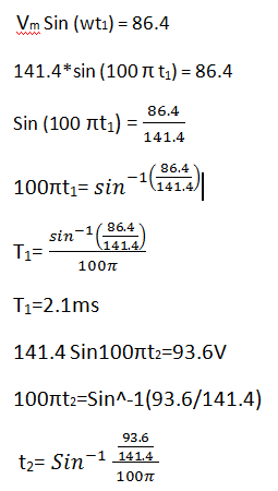
t2= 2.3ms
So the time duration for negative
inductor voltage is
∆t= t1+t2=
2.1ms+2.3ms=4.4ms
∆IL= 45*4.4/104
∆IL =
2A
For the conductor of Rectifier to
remain in continuous conduction mode, following condition must hold

So conductor will not go in
discontinuous conduction mode even if battery draws minimum current
So final values for rectifier’s
capacitor and inductor turns out to be
C=380uF & L=108mH
Now for buck converter

So we don’t have to worry for the
discontinuous conduction mode
The current wave form for the inductor
is given as follow
Using this waveform, the charge in the
capacitor can be calculated as

With this minimum current, the average
minimum current through the rectifier’s inductor is
ILmin = 1.15A
Which is safe limit range
Diode’s ratings for Buck converter

Switch ratings for buck converter
Is (av) =
K (12) = 2.136A
Is (peak) = IDpeak =12.07A
For Rectifier:
ID(av)
= IL(rectifier)/2 = 2.136/2
= 1.07 A
ID
(peak) = IL (rectifier) + 1/2∆IL
= 2.136 + ½(2)
ID (peak) = 3.136A

IDrms = 2.217A
So, Transformer VA rating is
VA = (2.217) x (100)
VAratings = 221.7VA
Maximum real power drawn by battery
VAratings = 221.7VA
Maximum real power drawn by battery
P = (16) x (12) = 192 W
The input Power factor when maximum
current is drawn
PF= 192/221.7= 0.866
Inverter
Design
What is an Inverter?
“A power inverter, or inverter, is an
electronic device or circuitry that changes direct current (DC) to alternating
current (AC). The input voltage, output voltage and frequency, and overall
power handling depend on the design of the specific device or circuitry.”
The second step of the design of uninterrupted power supply
is the design of inverter.
Components used for inverter design
Square Wave Generator:
H-Bridge circuit is used to generate
square wave for pulse transformer. The components chosen for this circuit are:

Switches:
The switches used for the square wave
generator circuit were NMOS IRF 320F with rating (110A, 55V).
The data sheet for IRF 320 is given as
follow:
Gate Driver:
The gate driver IC used for square
wave generator in our design is IR2101.
Switching Frequency for square wave generator:
10 kHz with k=0.495 & 0.5% dead
band.
Pulse Transformer:
What is Pulse
Transformer?
A transformer capable of operating over a wide range of
frequencies, used to transfer non-sinusoidal pulses without materially changing
their waveforms.
The power to the pulse transformer is turned on and off
using a switch (or switching device) at an operating frequency and pulse
duration that delivers the required amount of power. Consequently, the
temperature is also controlled. The transformer provides electrical isolation
between the input and output.
Pulse transformer designers usually seek to minimize voltage
droop, rise time, and pulse distortion. Droop is the decline of the output
pulse voltage over the duration of one pulse.
Why is Pulse Transformer used in our
Design?
Pulse transformer Design Parameters
Input to the Pulse Transformer is
provided by the square wave generator output. The input is a 1OKHz Square Wave
of 12V amplitude.
Now
In order to derive the maximum output load of 1000VA at 220v AC,
we need 331V peak AC voltage Supply. So, in order to meet our requirement we
need to design a pulse transformer to get output square waves of 311V amplitude.
As its output and input are square waves so, the RMS values of
input and output voltage and currents are the same as there amplitude so, we
need a pulse transformer of 1000VA rating.
The maximum current of pulse transformer is
Rated Input Current = 83.33A
Input current of pulse transformer passes through each switch, so
each switch of square wave generator should be able to bear 83.3A. We have
chosen IRF 320F for this purpose.
Pulse Transformer Design
Parameters:
Transformer Parameter Ratings:
VA rating= 1000VA
Input Current rating= 83.3A
Output Current rating= 3.2A
Input voltage rating= 12v
Output voltage rating= 311v
The design parameters of the core of
the pulse transformer are given as follow:
AcAὼ =
V=
311V
Kcu=
0.35
Bm =
0.3T
Irms=
3.2A
fs = 10 KHz
Now
From each data sheet of core we found
out that the Suitable ETD core is the ETD which has the parameter values of
So the number of turns for primary can
be calculated as given by the relation:
So by substituting the values of the
known parameters we can calculate the value of N1 as:
Which comes out to be
Which is
appropriate for our model.
Wire Selection for Primary and
Secondary of Pulse Transformer
For primary side
AWG gauge =
9
Diameter =
2.90576mm 0r 0.1144inches
Resistance/1000ft=
0.7927
Resistance/km=
2.598088
Max amperes
for power transmission = 19A
Max
frequency for 100% skin effect= 2050Hz
We have to
connect 5 such copper wires in parallel to get a wire for required frequency
range
We need 3
turns
As area of
core is 368mm2 for three turns on primary side we need wire of
length calculated as follow:
We know that
area of core is given by the relation Πr2 then by equating it to
the core area we get
Πr2 = 368mm2 or 0.368m2
r2 =
0.368m2 / π
r= 0.342259m
Now
Length of wire for one
turn is given as
2πr = 2*π*0.342259= 2.1504132 m
The length of wire for
N=78 is given by
L= 78*2.1504132=
167.732m
For Secondary Winding Wire Selection
AWG gauge = 16
Diameter = 0.0508 inch
= 1.29032 mm
Resistance/1000ft=
4.016
Resistance/km =
13.17248
Max amperes for Power
Transmission = 3.7A
Maximum frequency for
100% skin depth= 11 kHz
We need single wire of
this size for secondary winding of pulse transformer with 78 turns
Our core has a single
circular center leg on which we will wound both primary and secondary windings.
First the high voltage secondary winding with be wounded then an insulating
sheet will cover it and over the insulating sheet the primary windings will be
wounded.
Rectifier 2
Now here in case of a 1000VA output load 3.2A (Irms) current should be supplied by the pulse transformer so we have
RMS current rating of the diodes to be equal to 3.2A
Peak current rating= 3.2A?
Each diode conducts for half cycle of the square wave so
Inverter 2
Is (peak) = 6.4A
Is (rms)
= 4.545A
Here we have IRF840 as switch for inverter having current
rating of 8A and voltage rating of 500V
Its Turn ON delay= 14ns
Turn OFF delay= 49ns
Our switching period = 1/1000= 100us
% of turn on delay = 14n/100u * 100 = 0.014%
% of turn off delay = 49n/100u * 100= 0.49%
So, we need very small dead time of the order of 0.05% but
here we have introduced a dead time pf 0.5% which will definitely prevent any
chance of shoot through current.
Sr. No.
|
Component
|
No. of components
|
Price
|
1
|
IRF 840 (N-MOS switch(45/- each)
|
||
2
|
|||
3
|
IR 2101( gate driver circuit) (125/- each)
|
||
4
|
ETD Core (ETD 59/31/22)
|
800/-
|
|
5
|
1N5822 (Diode) (8/- per piece)
|
||
6
|
|||
7
|


0 comments:
Post a Comment